Introduction
Shift registers are one of the most important building blocks in digital electronics and sequential circuits. They are widely used for data storage, data transfer, serial-to-parallel conversion, parallel-to-serial conversion, timing applications, and digital signal manipulation. Almost every digital system, including microprocessors, microcontrollers, communication devices, and embedded systems, uses shift registers in some form.
A shift register is essentially a group of flip-flops connected in a specific way so that binary data stored in them can be shifted left or right in a controlled manner using clock pulses. Because shift registers operate based on clock signals and memory elements, they belong to the category of sequential circuits. Understanding shift registers is crucial for mastering digital electronics beyond basic combinational logic.
This article provides a deep and practical explanation of shift registers, their types, working principles, timing behavior, truth tables, and real-world applications, written in a WordPress-ready format.
What is a Shift Register?
A shift register is a sequential digital circuit that stores binary data and shifts it by one or more bit positions when a clock pulse is applied. It is constructed using flip-flops, usually D flip-flops, connected in series.
Each flip-flop stores one bit of data. On every active clock edge, the data moves from one flip-flop to the next, either to the left or to the right, depending on the design.
Key characteristics of shift registers include:
Clock-driven operation
Temporary data storage
Bit shifting capability
Serial and parallel data handling
Basic Structure of a Shift Register
A basic shift register consists of:
Multiple flip-flops connected in cascade
A common clock signal
Optional serial or parallel inputs
Optional serial or parallel outputs
The output of one flip-flop is connected to the input of the next, allowing data to move step by step with each clock pulse.
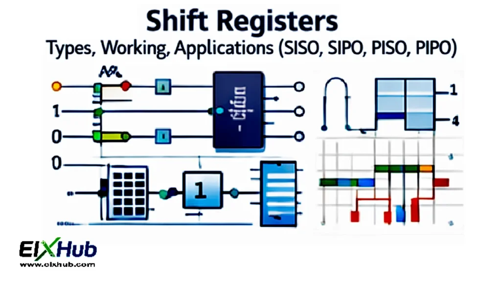
Types of Shift Registers
Shift registers are classified based on how data is entered and taken out.
Serial-In Serial-Out (SISO) Shift Register
Working Principle
In a Serial-In Serial-Out shift register, data is entered one bit at a time through a single serial input. With each clock pulse, the data shifts through the register, and the output is also obtained serially, one bit at a time.
Operation steps:
The first bit enters the first flip-flop
Each clock pulse shifts existing data to the next flip-flop
After n clock pulses, the first bit appears at the output
Characteristics
Simple structure
Used mainly for data delay and timing
Acts as a digital delay line
Applications
Time delay circuits
Serial data buffering
Synchronization of data streams
Serial-In Parallel-Out (SIPO) Shift Register
Working Principle
In a Serial-In Parallel-Out shift register, data is entered serially but retrieved in parallel. Each flip-flop output represents one bit of the stored data.
Operation steps:
Serial data enters one bit at a time
Clock pulses shift data through the register
After n clock pulses, all bits are available simultaneously at parallel outputs
Characteristics
Converts serial data into parallel data
Reduces number of input lines
Common in communication systems
Applications
Serial-to-parallel data conversion
LED and display drivers
Microcontroller input expansion
Parallel-In Serial-Out (PISO) Shift Register
Working Principle
In a Parallel-In Serial-Out shift register, multiple bits are loaded simultaneously into the register using parallel inputs. These bits are then shifted out one by one through a serial output.
Operation steps:
Parallel data is loaded using a load control signal
Clock pulses shift data out serially
One bit appears at the output per clock pulse
Characteristics
Parallel loading capability
Efficient data transmission
Requires fewer output lines
Applications
Parallel-to-serial conversion
Data transmission over single communication lines
Keyboard and sensor interfacing
Parallel-In Parallel-Out (PIPO) Shift Register
Working Principle
In a Parallel-In Parallel-Out shift register, data is loaded and retrieved in parallel. No shifting is required for data transfer, but the register can still shift data internally if designed to do so.
Characteristics
Fast data access
Simple control
Acts as a temporary data storage unit
Applications
Temporary data storage
Data buffering
Register files in processors
Bidirectional Shift Registers
Bidirectional shift registers can shift data either left or right depending on a control signal.
Applications include:
Arithmetic operations
Data manipulation
Serial communication systems
Universal Shift Register
A universal shift register is the most versatile type. It can perform:
Serial-in serial-out
Serial-in parallel-out
Parallel-in serial-out
Parallel-in parallel-out
Left shift and right shift
Universal shift registers are widely used in complex digital systems.
Timing Diagram and Operation
Shift registers are synchronous devices. Their operation depends on clock signals.
Key timing parameters:
Clock edge triggering
Setup time
Hold time
Propagation delay
Improper timing can lead to data loss or incorrect shifting.
Shift Registers as Sequential Circuits
Shift registers are sequential circuits because:
They use memory elements
Output depends on present input and previous state
They require clock signals
This distinguishes them from combinational circuits, which have no memory.
ICs Commonly Used for Shift Registers
| IC Number | Type | Description |
|---|---|---|
| 74LS95 | SIPO | Serial-in parallel-out |
| 74HC595 | SIPO | Popular for LED driving |
| 74HC165 | PISO | Parallel-in serial-out |
| 74LS194 | Universal | Bidirectional shift register |
| CD4015 | Dual SIPO | CMOS shift register |
Applications of Shift Registers
Data storage and buffering
Serial and parallel data conversion
LED matrix and display control
Digital clocks and timers
Communication interfaces
Arithmetic operations like multiplication and division
Data synchronization
Advantages of Shift Registers
Simple and reliable design
Efficient data handling
Low hardware complexity
Widely available ICs
Limitations of Shift Registers
Limited storage capacity
Speed depends on clock frequency
Not suitable for large data storage
Conclusion
Shift registers are fundamental components in digital electronics and sequential circuit design. By enabling controlled movement of binary data, they support data storage, transfer, and conversion between serial and parallel formats. Types such as SISO, SIPO, PISO, and PIPO shift registers serve different purposes in digital systems, from simple delays to complex communication interfaces. A solid understanding of shift registers is essential for working with microcontrollers, processors, and modern digital systems.
Image Reference Table
| Filename | Description | Alt Text |
|---|---|---|
| shift-register-basic.png | Basic shift register block diagram | Shift register block diagram |
| siso-shift-register.png | SISO shift register working | SISO shift register |
| sipo-shift-register.png | SIPO shift register diagram | SIPO shift register |
| piso-shift-register.png | PISO shift register diagram | PISO shift register |
| pipo-shift-register.png | PIPO shift register diagram | PIPO shift register |
| universal-shift-register.png | Universal shift register diagram | Universal shift register |
SEO Title
Shift Registers Explained – SISO, SIPO, PISO, and PIPO with Applications
Meta Description
Learn shift registers in digital electronics. Understand SISO, SIPO, PISO, and PIPO shift registers, working principles, ICs, timing, and real-world applications.